![]()
Faculty of Science and
Engineering,
Waseda University
早稲田大学 理工学術院
Important Notice重要なおしらせ

Topicsトピックス
Newsニュース

Eventsイベント
- MONTH
- 04
- DAY
- 27SAT
- YEAR
- 2024
| 月 | 火 | 水 | 木 | 金 | 土 | 日 |
|---|
| 1 | 2 | 3 | 4 | 5 | 6 | 7 |
| 8 | 9 | 10 | 11 | 12 | 13 | 14 |
| 15 | 16 | 17 | 18 | 19 | 20 | 21 |
| 22 | 23 | 24 | 25 | 26 | 27 | 28 |
| 29 | 30 | 1 | 2 | 3 | 4 | 5 |
年月日曜日のイベント
-
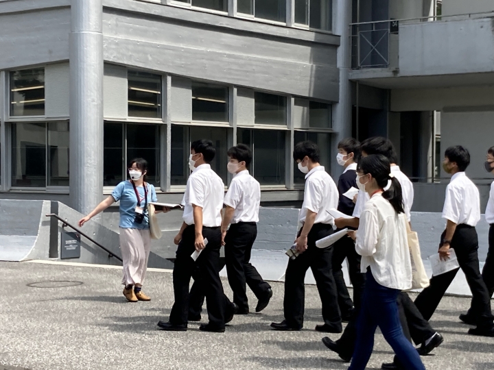
基幹理工学部
School of Fundamental Science and Engineering
-
基幹理工学研究科
Graduate School of Fundamental Science and Engineering
-
創造理工学部
School of Creative Science and Engineering
-
創造理工学研究科
Graduate School of Creative Science and Engineering
-
先進理工学部
School of Advanced Science and Engineering
-
先進理工学研究科
Graduate School of Advanced Science and Engineering
-

情報生産システム研究科
Graduate School of Information, Production and Systems
-
環境・エネルギー研究科
Graduate School of Environment and Energy Engineering
-

先端生命医科学センター(TWIns)
TWIns
-
理工学術院総合研究所
Waseda Research Institute for Science and Engineering
-

各務記念材料技術研究所
Kagami Memorial Research Institute for Materials Science and Technology
-

国際情報通信研究センター
Global Information and Telecommunication Institute
-
環境総合研究センター
Environmental Research Institute
-
情報生産システム研究センター
Information, Production and Systems Research Center